Semiconductor and Display

Lasers have the advantage of being as small as the submicron order of focus, allowing for more meticulous microprocessing of wafers and the ability to process small parts.
Even at modest pulse energy levels, high energy densities can be obtained for efficient material processing.

GZTECH high-quality mopa pulsed fiber laser sources used for single and double mesa glass passivated diode wafers in the semiconductor manufacturing industry; single and double mesa thyristor wafers; IC wafer cutting and other semiconductor wafer cutting and dicing.

Industry Application

Marking

Cutting

Marking

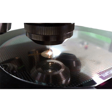
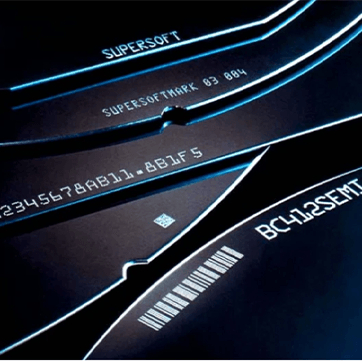
Laser marking is a marking method that uses a high-energy density laser beam to act on the target to cause physical or chemical changes on the target surface, thereby obtaining a visible pattern. A high-energy laser beam is focused on the surface of the material, causing the material to vaporize rapidly, forming pits.
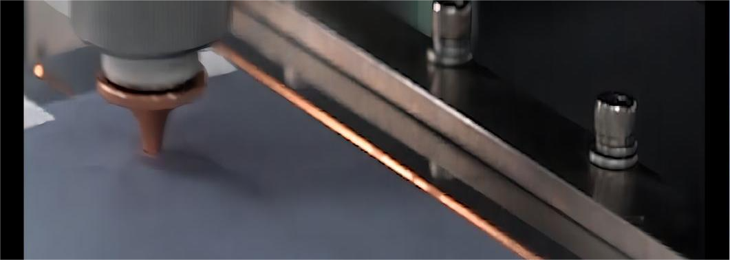


Cutting

In the process of wafer processing, making a laser identification code at a specific position of the wafer can effectively enhance the traceability of the wafer, and also provide a certain convenience for production management. At present, making laser identification codes on wafers has become a potential industry standard, and is widely used in silicon and germanium materials.


Related Products

 
×

Contact Us

×

Inquire

*Name
*Email
Company Name
Tel
*Message