

Copyright © 2022 Wuhan Guangzhi Technology Co., Ltd All rights reserved.Site MapDesigned by 
Welcome:GZTECH
Welcome:GZTECH
Reducing costs and increasing efficiency is the eternal pursuit of the PV industry. Large-size silicon wafers can not only reduce the number of slicing times, reduce the cost of slicing and the cost per watt of silicon wafers, but also speed up the production speed from silicon wafers to modules, thereby reducing production and operation costs. With the reduction of photovoltaic costs, according to the forecast of CPIA, China's newly installed PV capacity will exceed 100GW for the first time in 2024, and the growth rate of demand for PV industry certainty in the next decade may exceed the rate of price reduction and enter a sustained and stable expansion phase.
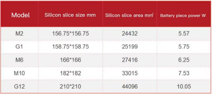
Dimensions of different types of silicon wafers
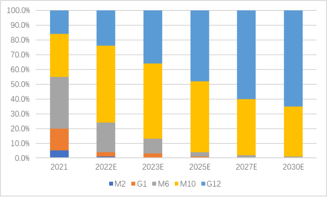
Forecast of the proportion of silicon wafer shipments with different specifications
The current of the cell is proportional to the area of the silicon chip. Large-sized cells are bound to be accompanied by high currents. After the cells are packaged in series into modules, the power loss is proportional to the square of the current. In order to reduce the power loss caused by the current, the prepared large-size cell can be divided into two slices or three or even five slices, and then packaged into half or one-third slice components, or even one-fifth slice shingled components.
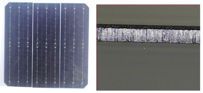
At present, lasers are commonly used to scribe and cut the entire battery sheet. The traditional laser scribing machine uses a pulse laser to process a slit through the surface with a vibrating mirror on the back of the cell, and then uses a mechanical method to split the cell along the cutting line. There are two disadvantages for this method: one is the laser thermal ablation process will leave a large amount of thermal damage (80-120μm) on the cut surface, which will reduce the mechanical strength of the cell; second, for large-size silicon wafers, it is very easy to break, and this method is basically not suitable for large-size silicon wafers.
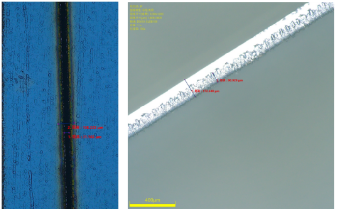
Conventional scribing effect of pulsed laser
In the development of large, thin and efficient cell module technology, laser non-destructive cutting, as a new type of photovoltaic cell cutting technology, has the advantages of size compatibility, no mechanical damage, high efficiency, and less pollution,and is currently the main way to slice cells.
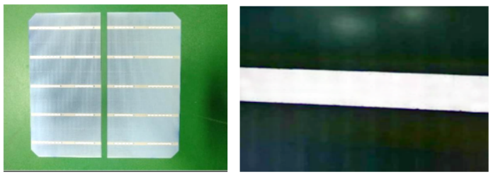
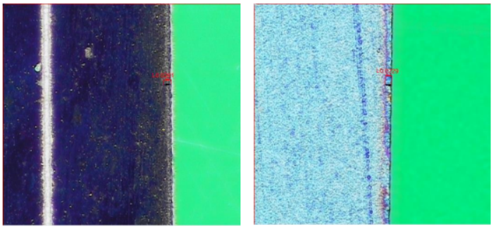
Non-destructive scribing effect
In the early stage, GZTECH used 70W MOPA with 300W continuous single-mode for non-destructive cutting of silicon cells and achieved good results. The surface is basically free from heat effects, and the cross-section is smooth and has no damage. However, some customers do not have high requirements for slicing, and expect a low-cost large-size cell slicing solution.
Combining the advantages and disadvantages of the conventional silicon cell slicing method and the non-destructive cutting method, GZTECH started from the characteristics of the laser, conducted in-depth process research, and developed a set of cell slicing solutions with simple structure and low equipment cost. This solution uses the cutting head with auxiliary gas to cut through the silicon wafer at a speed of 600mm/s.
Compared with the traditional galvanometer slicing method, this method has a less thermal impact (<30 μm), neat cross-section, high efficiency, and can be applied to silicon cells of various sizes. Compared with non-destructive cutting, this scheme is simple in structure and low in cost, but the effect will be slightly worse. Adopting the 300W continuous single-mode laser of GZTECH plus cutting head slice way, the effect is better than the traditional galvanometer fragmentation and worse than non-destructive cutting, but the cost is controllable, which meets the core demand of "reducing costs and increasing efficiency" in the photovoltaic industry.
GZTECH is a leading supplier of advanced industrial laser products for precision manufacturing. In order to meet the needs of various customers, we are building a layout with Wuhan headquarters as the center and five major offices serving the whole country. At present, there are three major offices in Shenzhen, Suzhou and Jinan, all of which can provide samples for customers. We welcome customers to discuss the development of new laser processes with us.
 Promote laser to be a fundamental tool for smart manufacturing

Copyright © 2022 Wuhan Guangzhi Technology Co., Ltd All rights reserved.Site MapDesigned by
By continuing to use the site you agree to our privacy policy Terms and Conditions.